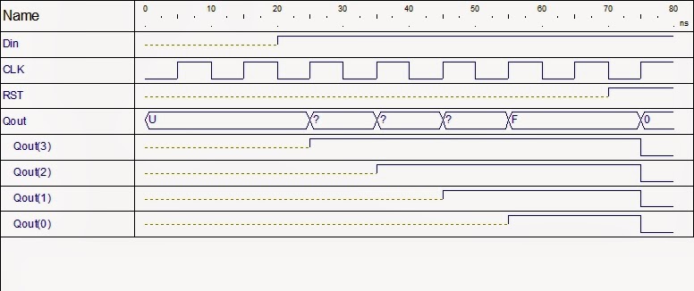
A 4-bit shift register design in VHDL is illustrated with waveform output. The shift register is made of 4 D Flip Flop. Data enters 1 bit at a time into the first D Flip Flop which is then shifted along the cascaded shift register.
D Flip Flop:
The D Flop Flip is the basic unit of the 4 bit shift register. It is a synchronous flip flop with clock and reset input. The input for data is D and the output is Q.

D Flip Flop:
library ieee;
use ieee.std_logic_1164.all;
entity dff is
port(
D : in std_logic;
CLK : in std_logic;
RST : in std_logic;
Q : out std_logic
);
end dff;
architecture dff_arch of dff is
begin
process (CLK)
begin
if CLKevent and CLK=1 then --CLK rising edge
if RST =1 then --synchronous RESET active High
Q <= 0;
else
Q <= D;
end if;
end if;
end process;
end dff_arch;
Shift Register:
The shift register below instantiates the above D Flip Flip 4 times for the 4 Flip Flops. The input to the register is Din which is feed to the first D Flip Flop. The out of the shift register is Qout.
 Shift Register Code:
library ieee;
use ieee.std_logic_1164.all;
entity register_design is
port (
Din : in std_logic;
CLK : in std_logic;
RST : in std_logic;
Qout : out std_logic_vector(3 downto 0)
);
end register_design;
architecture register_arch of register_design is
signal q0, q1, q2, q3 : std_logic;
begin
ff1: entity work.dff(dff_arch)
port map (
D => Din,
CLK => CLK,
RST => RST,
Q => q0
);
ff2: entity work.dff(dff_arch)
port map (
D => q0,
CLK => CLK,
RST => RST,
Q => q1
);
ff3: entity work.dff(dff_arch)
port map (
D => q1,
CLK => CLK,
RST => RST,
Q => q2
);
ff4: entity work.dff(dff_arch)
port map (
D => q2,
CLK => CLK,
RST => RST,
Q => q3
);
Qout <= q0&q1&q2&q3;
end register_arch;
Testbench Code:
library ieee;
use ieee.std_logic_1164.all;
entity register_design_tb is
end register_design_tb;
architecture TB_ARCHITECTURE of register_design_tb is
component register_design
port(
Din : in STD_LOGIC;
CLK : in STD_LOGIC;
RST : in STD_LOGIC;
Qout : out STD_LOGIC_VECTOR(3 downto 0) );
end component;
signal Din : STD_LOGIC;
signal CLK : STD_LOGIC;
signal RST : STD_LOGIC;
signal Qout : STD_LOGIC_VECTOR(3 downto 0);
begin
UUT : register_design
port map (
Din => Din,
CLK => CLK,
RST => RST,
Qout => Qout
);
CLK_GEN: process
begin
CLK <= 0;
wait for 5 ns;
CLK <= 1;
wait for 5 ns;
end process;
stimuli : process
begin
Din <= 1 after 20 ns;
RST <= 1 after 70 ns;
Din <= 1 after 90 ns;
wait;
end process;
end TB_ARCHITECTURE;
configuration TESTBENCH_FOR_register_design of register_design_tb is
for TB_ARCHITECTURE
for UUT : register_design
use entity work.register_design(register_arch);
end for;
end for;
end TESTBENCH_FOR_register_design;
Waveform

In the waveform graph above, the data input is 1 at 20 ns which is propagated through the D flip flops as shown by Qout(3), Qout(2), Qout(1) and Qout(0). At 70 ns Reset signal RST is applied which puts all the D flip flop states to 0.
D Flip Flop:
The D Flop Flip is the basic unit of the 4 bit shift register. It is a synchronous flip flop with clock and reset input. The input for data is D and the output is Q.

D Flip Flop:
library ieee;
use ieee.std_logic_1164.all;
entity dff is
port(
D : in std_logic;
CLK : in std_logic;
RST : in std_logic;
Q : out std_logic
);
end dff;
architecture dff_arch of dff is
begin
process (CLK)
begin
if CLKevent and CLK=1 then --CLK rising edge
if RST =1 then --synchronous RESET active High
Q <= 0;
else
Q <= D;
end if;
end if;
end process;
end dff_arch;
Shift Register:
The shift register below instantiates the above D Flip Flip 4 times for the 4 Flip Flops. The input to the register is Din which is feed to the first D Flip Flop. The out of the shift register is Qout.

library ieee;
use ieee.std_logic_1164.all;
entity register_design is
port (
Din : in std_logic;
CLK : in std_logic;
RST : in std_logic;
Qout : out std_logic_vector(3 downto 0)
);
end register_design;
architecture register_arch of register_design is
signal q0, q1, q2, q3 : std_logic;
begin
ff1: entity work.dff(dff_arch)
port map (
D => Din,
CLK => CLK,
RST => RST,
Q => q0
);
ff2: entity work.dff(dff_arch)
port map (
D => q0,
CLK => CLK,
RST => RST,
Q => q1
);
ff3: entity work.dff(dff_arch)
port map (
D => q1,
CLK => CLK,
RST => RST,
Q => q2
);
ff4: entity work.dff(dff_arch)
port map (
D => q2,
CLK => CLK,
RST => RST,
Q => q3
);
Qout <= q0&q1&q2&q3;
end register_arch;
Testbench Code:
library ieee;
use ieee.std_logic_1164.all;
entity register_design_tb is
end register_design_tb;
architecture TB_ARCHITECTURE of register_design_tb is
component register_design
port(
Din : in STD_LOGIC;
CLK : in STD_LOGIC;
RST : in STD_LOGIC;
Qout : out STD_LOGIC_VECTOR(3 downto 0) );
end component;
signal Din : STD_LOGIC;
signal CLK : STD_LOGIC;
signal RST : STD_LOGIC;
signal Qout : STD_LOGIC_VECTOR(3 downto 0);
begin
UUT : register_design
port map (
Din => Din,
CLK => CLK,
RST => RST,
Qout => Qout
);
CLK_GEN: process
begin
CLK <= 0;
wait for 5 ns;
CLK <= 1;
wait for 5 ns;
end process;
stimuli : process
begin
Din <= 1 after 20 ns;
RST <= 1 after 70 ns;
Din <= 1 after 90 ns;
wait;
end process;
end TB_ARCHITECTURE;
configuration TESTBENCH_FOR_register_design of register_design_tb is
for TB_ARCHITECTURE
for UUT : register_design
use entity work.register_design(register_arch);
end for;
end for;
end TESTBENCH_FOR_register_design;
Waveform

In the waveform graph above, the data input is 1 at 20 ns which is propagated through the D flip flops as shown by Qout(3), Qout(2), Qout(1) and Qout(0). At 70 ns Reset signal RST is applied which puts all the D flip flop states to 0.
0 comments:
Post a Comment